
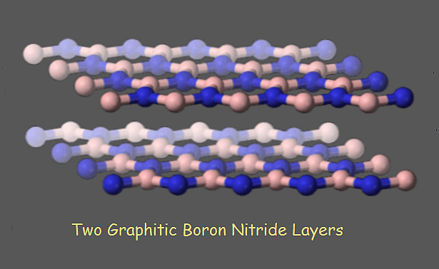
 Boron, like many other elements, forms nitrides. These nitrides can assume a variety of crystalline structures. One of those varieties consists of atoms in hexagonal array, layered in sheets. It is hexagonal boron nitride, or h-BN. A sheet of h-BN outwardly resembles a sheet of graphene. For this reason, some refer to it as graphitic boron nitride.
We shall see that, despite a considerable similarity in appearance on papers, there are major differences between graphene and h-BN as well. Very significant differences.
Graphene Vs. Hexagonal Boron Nitride
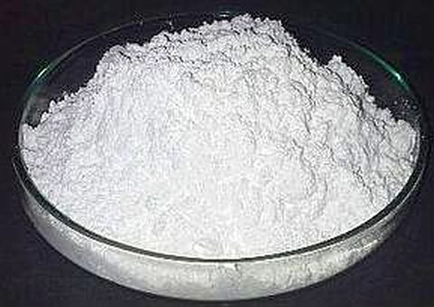
Atomic spacing within a single layer of hexagonal boron nitride varies slightly from that of a sheet of graphene. As a result, graphene is black, while h-BN is white!
Graphene’s C–C bonds are non-polar in nature. Hexagonal boron nitride’s B–N bonds are highly polar. Graphene is an excellent electrical conductor, whereas hexagonal boron nitride is an electrical insulator, due to its wide band gap¹, although it is a thermal conductor.
If a sheet of graphene is placed upon a sheet of h-BN, the atoms do not line up vertically. And, as might be expected from their relative polarities, the two substances do not interact, chemically.
This enables a sheet of h-BN to serve as a substrate for a sheet of graphene. But why would one want to construct such an open-faced sandwich?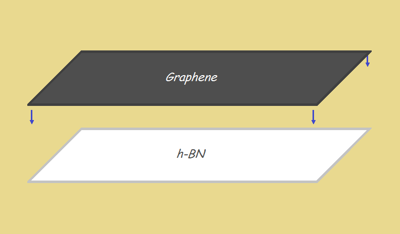
Why, Indeed?
We live in a 3D world. However, with advancement in computers and other electronic devices, component size is crucial. This includes thickness, and devices are under investigation that approximate 2D. Hexagonal boron nitride seems an ideal choice for such diminutive substrates.
Comparison to Thick Film and Thin Film Technologies
Thick Film: From 1970-1971, the author was involved in thick film production at Electro-Science Laboratories. Small and moderately thin ceramic substrates (usually alumina) are screen-printed with a layer of one or more thick films, consisting of conductors, resistors, and dielectric pastes.
The substrates were kiln-fired, sometimes in a specialty atmosphere, with carefully controlled thermal cycling.
Thin Film: Much the same concept, thin-film deposition often involves atomic deposition methods, producing yet a thinner layer of material on a substrate. Often this involves the vapor phase. Sputtering1 was one popular way of depositing a thick film.
The Need for Smaller
Just when a product is developed that seems to fill the bill, newer, stricter requirements call for yet newer, more capable methodologies. As a substrate material, h-BN seems a superlative choice.
In addition to the previously mentioned physical characteristics of h-BN, we should add its suitability as a dielectric. Clearly research scientists have their eye on hexagonal boron nitride as a most promising, multiple use, raw material.
1 See University of Calgary: Energy Education: Band Gap
2 See AJA International Inc: What is Sputtering?
Note: You might also enjoy Graphene Properties, Applications, and Production
References:
- ACS Publications: Graphite and Hexagonal Boron-Nitride have the Same Interlayer Distance. Why? [Abstract – 2012]
- ACS Publications: Large-Area Monolayer Hexagonal Boron Nitride on Pt Foil [Abstract – 2014]
- Science Direct: Journal of Materials Science & Technology: Recent Progress on Fabrications and Applications of Boron Nitride Nanomaterials: A Review
- Semantic Scholar: Synthesis and characterization of hexagonal boron nitride film as a dielectric layer for graphene devices.
Hmm, that has provoked a thought in the science fiction story part of my brain! I must let it sit and ferment somewhat.